Projets de recherche

Méga Sète
Déploiement de la première ferme photovoltaïque offshore pré-commerciale de 1MW en méditerranée française
Partenaires :
SolarinBlue, Technip Energies France, Sorbonne Universite - L Observatoire Oceanologique de Banyuls-Sur-Mer
Financé par :

Halt O’Plast
Développement d'une technique de captation de microplastiques en milieu aqueux basée sur un couplage électrostatique/micro-fluidique
Partenaires :
Financé par :
Actualités GEMS
02/07/2024
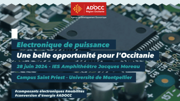
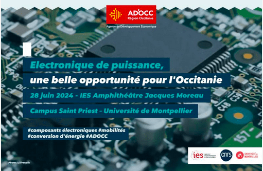
Le Colloque Electronique de Puissance # 3: un succès pour l’IES et AD’OCC
Le Colloque Electronique de Puissance s’est déroulé comme prévu (et annoncé par Touléco), ce vendredi 28 juin à l’IES, avec…
En savoir plus
30/05/2024
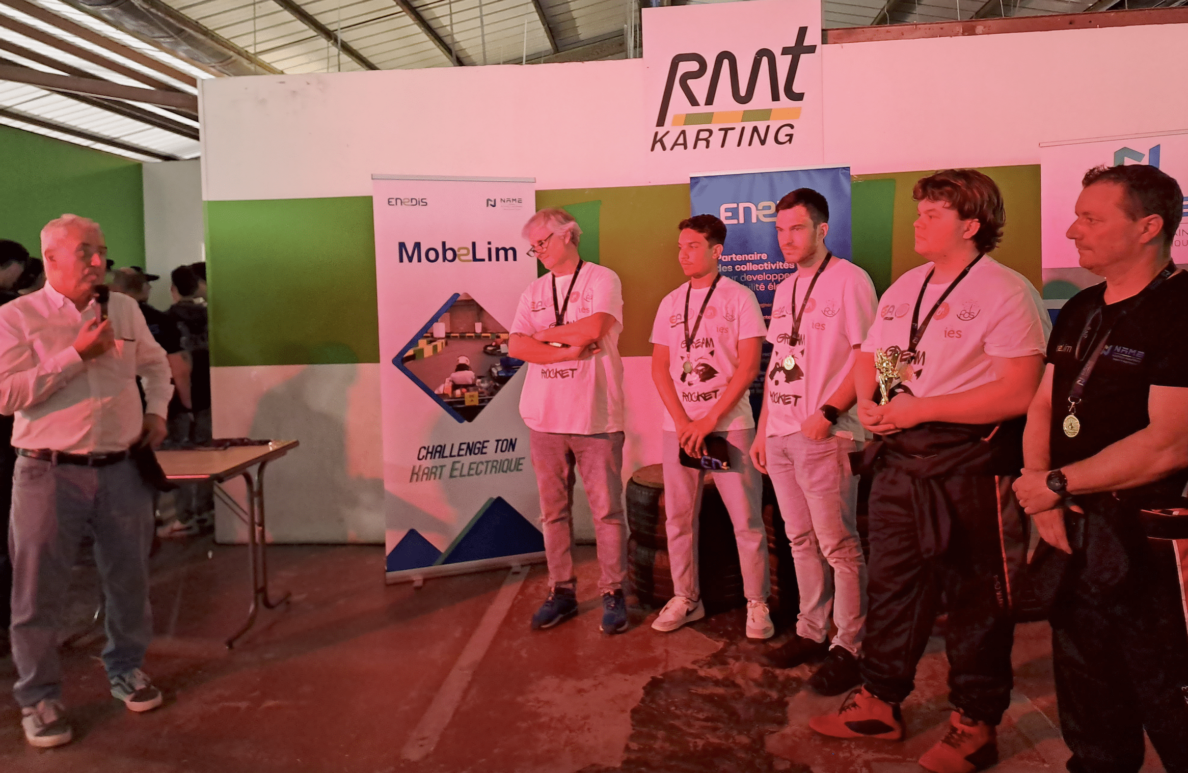
Le succès du kart électrique de l’UM/IES
Un kart électrique a été entièrement développé au sein du département d’enseignement EEA (Electronique, Electrotechnique et Automatique) de la faculté…
En savoir plus
16/05/2024
Colloque Electronique de Puissance à l’IES le 28 juin
Après les deux premières éditions de ce Colloque à Toulouse et à Tarbes en 2023, c’est au tour de l’IES…
En savoir plus